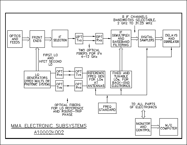
Figure 1: Overall block diagram of the MMA System
A. R. Thompson
Nov. 6, 1997
This report is concerned with the MMA receiving system and is based upon discussions of the MMA systems group. The part of the system considered here includes the signal paths from the outputs of the front ends to the digital samplers, and the local oscillator (LO) system, but does not include details of the front ends, the digital delays or the correlator. The system shown is designed to work with optical fiber transmission of IF signals in analog form from the antennas to the Electronics building at the site. Some discussion on the choice of analog or digital transmission can be found in MMA Memo.142. The digital alternative is not ruled out. It remains under study and will be discussed in a later memorandum. With digital transmission practically all of the system discussed here would remain, but some of it would be relocated to the antennas and some further hardware would be required. It is clear that digital transmission would result in a more expensive and complicated system. Measurements with the two-element prototype system should be used to help verify the final choice of analog or digital transmission.
At this point in the project development the intention is to provide a broad outline of the proposed system. The diagrams indicate the signal flow through the system by showing mainly filters, mixers and switches. Amplifiers, attenuators, isolators, etc. will be added as design details are developed, and precise frequencies of filters, LOs, etc. may require minor adjustments. A simplified block diagram of the overall system is shown in Fig. 1. Components at the left-hand side of the optical fibers in the IF and LO paths are located at the antennas and those at the right-hand side are in the Electronics building which also contains the delay system and correlator. Signals from the Cassegrain feeds are converted to IFs in the front ends. There are approximately ten front ends covering the total observing range of the MMA. The IF signals from the front end that is selected at any time are transmitted to the Electronics building in the form of two 8 GHz-wide analog bands. At the Electronics building the signals are split into eight baseband channels and filtered, digitized, delayed and correlated. A frequency standard provides the reference frequencies for various local oscillators and for timing of the digital units. For the LOs at the antennas, frequencies are generated at the Electronics building and are transmitted to the antennas on optical fibers. Another fiber may be provided for measurement of the round-trip phase. Appropriate phase switching and fringe-frequency phase rotation are inserted through to LO system. A monitor and control system interacts with all parts of the electronics.
Signal Paths at the Antennas
Figure 2 shows the system at the antennas. The front ends for frequencies above approximately 115 GHz will use SIS mixers and those below 90 GHz will use HFET amplifiers. The choice for the 90-115 GHz has not yet been made. The SIS mixers will have separate outputs for the upper and lower sidebands. Thus there will be four IF outputs from each SIS front end, to provide signals for two polarizations and two sidebands. Each output goes to one of four 1x10 switches. An IF band spanning 4 to 12 GHz (i.e. a bandwidth of 8 GHz) for each of the two polarizations can be accommodated. SIS mixers used by NRAO currently have IF bandwidths no greater than 2 GHz, but a mixer with a 4 GHz IF bandwidth and good noise temperature has been demonstrated by Padin et al. (1996) using an IF stage integrated with the mixer. It is felt that 8 GHz bandwidth is an achievable goal within the construction period of the MMA. However, in the shorter term the noise temperature of SIS front ends matched to a 4 GHz bandwidth may be better than those matched to the full 8 GHz bandwidth. Thus, instead of two 8-GHz-wide bands it may be preferable to use four 4-GHz-wide bands from each SIS front end (i.e. both polarizations for upper and lower sidebands) in order to maximize the sensitivity. By means of the four 1x2 and two 1x3 switches shown in Fig. 2, the input to each optical transmitter can be selected to come from either one 4-12 GHz front end output or two 4-8 GHz front end outputs, one of the latter being converted to 8-12 GHz for transmission on the fiber. Note that a rearrangement of the components shown plus the addition of two optical transmitters would allow the signals to be transmitted as to the building as four bands of width 4 GHz, although it is not expected that there will be any difficulty in transmitting 8 GHz bandwidths over fiber lengths up to 20 km.
The HFET-amplifier front ends have separate outputs for the two polarizations. The maximum bandwidth of any of the HFET front end is approximately 26 GHz. The first IF for the HFET front ends is 14 to 22 GHz, so there is a frequency space of 28 GHz between the upper and lower sideband responses at the mixer that converts to the first IF. Thus for most HFET front ends it should be possible to avoid an image response if a filter is included to confine the amplifier response to the nominal band. If necessary the LO can be on the low side when the required IF band is in the lower half of the HFET band and on the high side when the required band is in the upper half of the HFET band, to keep the image response further away from the amplifier passband. Note that the IF band 14-22 GHz is about as low in frequency as is possible to use while avoiding direct feed through to the 4-12 GHz band. For reasons of cost it is preferable to keep intermediate frequencies as low as possible, but the IF bandwidths required place lower limits on the frequencies because of the need to avoid image responses, etc.
The arrangement of switches shown in Fig. 2 is one of several possibilities and the final system design will have to take into account the availability and cost of different types of switches. Some modes of operation of the array may require continuous switching between two front ends at intervals of ~10 sec. Specified lifetimes of some mechanical switches are ~106 cycles, which could be reached after about 100 days of such operation. Thus solid state switches may be necessary.
IF Signal Processing at the Electronics Building
Each of the 4-12 GHz IF bands is demultiplexed into four 2 GHz-wide bands when received at the Electronics building. Figure 3 shows the circuitry for the signal from one optical fiber. Two such Demultiplexer units are required for each antenna. The basic reason for this frequency demultipexing is that the maximum clock frequency of the samplers is 4 GHz. All four 2 GHz-wide bands are converted to the same frequency (2-4 GHz) so that in the next stage of signal processing they can be handled by identical baseband units. The 2-4 GHz filters at the outputs of this unit require a sharp response at the 4 GHz edge, since when using the full bandwidth the signals are converted to baseband with the 3.2-5.2 GHz LO (see Fig. 4) tuned to 4 GHz in the Baseband Converters. The switching network allows the four outputs to be connected to four Baseband Converter inputs in any manner desired. For example, all four Baseband Converters may be connected to one 2 GHz-wide IF band if one wishes to study four narrow lines that all lie within the same 2 GHz-wide band. The switching network could be implemented by a combination of four 4-way power dividers and four single-pole, 1x4 switches.
In the Baseband Converter unit in Fig. 4, the input signal at 2-4
GHz is converted to the baseband range and filters are provided for
selection of bandwidths from 2 GHz down to 31.25 MHz in steps of a
factor of two. The 3.2-5.2 GHz LO at the first frequency conversion
is tunable to allow the response of the Baseband Converter to be set
at any part of the 2-GHz-wide IF input band. In designing the
Baseband Converter, it was decided to use a system involving a number
of frequency conversions with filters chosen to reject the unwanted
sideband responses, rather than using a sideband-separating mixer
scheme because the latter, although simpler, does not provide
sufficient rejection of unwanted sidebands. The widest bandwidth,
0.1-2.0 GHz, may contain a small unwanted component which arises from
conversion of residual frequencies in the 4 GHz skirt of the 2-4 GHz
filters. This component consists of frequencies that are folded into
the low frequency end of the baseband by the conversion process, and
the filter response rejects frequencies below 0.1 GHz to minimize such
unwanted signals. (The 0.1 GHz filter edge is a nominal value at this
time and may require adjustment when the response of the 2-4 GHz
filters in the demultiplexing unit (Fig. 3) is specified in detail.)
The 1-2 and 1-1.5 GHz filters are far enough away from the low end of
the 0-2 GHz baseband to be free from such unwanted components.
Similarly the two frequency bands following each of the 1.5 GHz and
375 MHz LOs are well above zero frequency and will not include
unwanted components from spectrum fold-over at an LO frequency.
Listed below are the bandwidth of each filter, the frequency range of
the passband as seen at the output of the first mixer (the one with
the 3.2-5.2 GHz LO), and the tuning range of the LO which just covers
the 2-4 GHz input band in each case. Images fall above 4 GHz in all
cases.
| Bandwidth | Filter response as seen | LO tuning range |
| at output of first mixer | ||
| 1.9 GHz | 0.1-2.0 GHz | 4.0 GHz |
| 1.0 GHz | 1.0-2.0 GHz | 4.0-5.0 GHz |
| 500 MHz | 1.0-1.5 GHz | 3.5-5.0 GHz |
| 250 MHz | 1.0-1.25 GHz | 3.25-5.0 GHz |
| 125 MHz | 1.125-1.25 GHz | 3.25-5.125 GHz |
| 62.5 MHz | 1.1875-1.250 GHz | 3.25-5.1875 GHz |
| 31.25 MHz | 1.1875- 1.21875 GHz | 3.2187-5.1875 GHz |
The fractional bandwidths of the filters, other than the two widest ones, are in the range 0.4 to 0.67. Note that if the chosen output band comes from one of the three widest filters, the input of the 1.5 GHz LO signal to the module should, if necessary, be turned off to prevent pickup of this LO frequency in the earlier filters. Similarly, unless one of the two narrowest bandwidths is being used the 375 MHz signal should be switched. The filtered outputs are sampled at a 4 GHz clock rate and digitized. The digital data go to the delay and correlator systems and redundant samples for the bandwidths of 1 GHz and less are removed as necessary at an appropriate stage. Eight Baseband Converter units are required for each antenna.
Total Power Observations and Signal Level Control
In the IF system at the antennas (Fig. 2) detectors are shown which measure the IF signal level in the 4-GHz-wide and 8-GHz-wide bands at the inputs to the optical transmitters. In the Baseband Converter (Fig. 4) a detector is shown which measures the level of the signal going to the digital sampler. These detectors perform two functions. First, they can be used for total power measurements. Those at the antenna would be used for wide-band continuum measurements. For total power measurements in spectral line mode the autocorrelation outputs of the correlators are required. Note that at the antennas it is possible to make total power measurements on all four 4-12 GHz outputs of an SIS front end simultaneously, thus making use of twice the bandwidth that is available in interferometer mode.
The second use of the detectors is to check the IF level at two points where the level is critical. One of these is the inputs to the optical transmitters in which nonlinearity can occur if the level is too high, and loss of SNR can occur if the level is too low. The other point is the sampler input where it is necessary to know the reference levels in terms of the rms input noise level. In either case some range of level variation is acceptable, and it is considered that use of an ALC loop may be undesirable. However, a variable attenuator or a variable-gain amplifier (not shown in the figures) will be included in the signal path ahead of each detector. These gain controls and the detector outputs will be accessed through the monitor and control (M/C) system. Thus various control schemes including adjustment in discrete steps, full ALC, sample-and-hold, etc. can be implemented through a control computer. If on-the-fly mapping or subreflector nutation are used in observing, then it may be necessary to measure the gain for a particular reference direction of the beam.
As a means of calibrating the system noise and gain, it is proposed to inject a controlled level of noise into the front ends in a switched sequence including zero additional noise and two levels chosen to increase the system noise by a few percent. An arrangement involving thermal sources radiated from a small aperture in the antenna subreflector is being investigated at Berkeley.
Phase Switching and Fringe Rotation
Although SIS mixers incorporating sideband separation are being developed for the MMA, it is expected that it will be possible to achieve only 10-15 dB of isolation between the sidebands. This is sufficient to eliminate the noise from the unwanted sideband to a satisfactory degree. However, spectral dynamic range at least as high as 40 dB is desirable, so it is also necessary to include sideband separation either by 90 deg phase switching or by a frequency offset scheme suggested by B. Clark. Either of these schemes must be applied to the first LO. It is also generally useful to incorporate 180 deg phase switching to reduce effects such as unsymmetrical offsets in the sampler reference levels and spurious responses from unwanted signals that infiltrate the IF stages.
A complication in the use of phase switching with the MMA occurs because of the requirement for integration times as short as 10 ms. For the longest baselines which we take to be 10 km, and for a source at a low elevation angle, the difference in the times at which an incident wavefront reaches different antennas can be as much as 33µs. Now to preserve the orthogonality of the Walsh functions the switching transitions must be coincident at the correlator input, i.e. after the compensating delay. Thus, at the points where the Walsh function switching is introduced, it is necessary to introduce time offsets of up to 33µs into the transitions. These offsets depend upon the position of the antenna concerned within the array, and the position of the source on the sky. (In the VLA the corresponding timing differences all fall within the 1 ms intervals of the waveguide cycle in which the IF signals are switched off, and can thus be ignored.) For the MMA, if the shortest switching interval of the Walsh functions is much longer than 33µs, say 33ms, then the timing offsets of the Walsh functions could probably be ignored. For a number of antennas between 64 and 128 the duration of a complete Walsh cycle is 128 times the shortest switching interval, and it is necessary to integrate for integral numbers of Walsh cycles if the phase switching is to work efficiently. Thus the requirement for ignoring the timing offsets of the Walsh functions would be integration times longer than ~4 sec. So the conclusion is that if Walsh function phase switching is used on the MMA, time offsets of the transitions are required. This is not a big problem, but it results in a complication of the software that one would prefer to avoid.
For the sideband separation the 90 phase switching can be avoided by using the frequency offset scheme mentioned above. To explain this scheme, consider first just two elements of the array. Let the natural fringe frequencies (i.e. fringe frequencies with no fringe rotation applied) be fnl and fnu for the lower and upper sidebands respectively. At the first LO of one of the antennas an offset f1 is applied so that the two fringe frequencies become (fnl + f1) and (fnu + f1). The frequency f1 is chosen such that f1 + (fnl + fnu)/2 = n/(2t), where n is an integer and t is the integration time between correlator data dumps. (Note that the natural fringe frequencies for the MMA vary from zero to about 600 kHz, so f1 may have to be positive or be negative, i.e. the natural frequency may have to be increased or reduced.) Then at a later LO, which in the present plan is the LO at the first mixer of the Baseband Converter, we introduce a second frequency offset to convert to zero frequency the fringes of the sideband that we want to use. For example, if we want to keep the upper sideband then this second LO offset is -(fnu + f1). The effect on the lower sideband is to offset its frequency in the opposite direction, that is, the frequency of the lower sideband fringes becomes (fnl + f1) + (fnu + f1) = n/t. The lower sideband fringes then integrate to zero in time t. To apply this scheme to the full array the value of n must be different for each antenna, and can run from 0 to (Na -1), where Na is the number of antennas. For t~10 ms and t~Na 100 the fringe frequencies of the unwanted sideband at the correlator output are of order 1 kHz and no constraint is placed on the rate of correlator data dumps.
The fringe-offset scheme for removing the unwanted sideband has other advantages over the process of fringe separation by 90 phase switching. It can be implemented by using the fringe rotators that are required in any case to bring the fringe frequency of the wanted sideband to zero, so no extra hardware is required. Also, the variation with time of the differential path lengths to the antennas, which in the case of Walsh function switching requires timing offsets, is in this scheme taken care of by the fringe rotation. The unwanted sideband is lost in the integration, but this is not a problem since we are planning to use sideband-separating SIS mixers so any IF signal contains only one sideband at full sensitivity, the other being reduced by at least 10 dB.
Unfortunately there does not appear to be any frequency-offset method of implementing the 180 phase switching, so Walsh-function switching with timing offsets to compensate for the different path lengths of the incoming wavefront remains the complete solution. If the phase switching is necessary only to correct for non-symmetrical quantization thresholds, then it would be possible to replace it by automatic control of the threshold levels. For four-level sampling the dc level of the sampled waveform would be adjusted to equalize the total numbers of positive and negative samples, and the quantization levels would be adjusted to equalize the numbers of positive and negative high-level counts. Counters for the four sampling levels would provide inputs to digital-to-analog converters to provide the dc levels. Such a scheme may be examined as part of the two-element prototype testing. Removal of the phase switching would occur just after the digital samplers by sign reversal of the appropriate samples as controlled by the phase-switching Walsh function, and is shown in Fig. 4.
The fringe rotators may also be used for fine adjustment of the Doppler correction, the magnitude of which may be as large as 100 MHz at 800 GHz. Thus the range of the offsets from the fringe rotator should be as wide as the narrowest tuning interval provided by any other LO, to provide complete frequency flexibility. Alternatively, Doppler shifts can be removed by interpolation of the spectra at the correlator output.
The Local Oscillator System
Two version of the LO system are shown in Figs. 5 and 6. Figure 5 shows the system with a conventional multiplier scheme for the first LO, and Fig. 6 shows the photonic system for the first LO which will offer significant advantages if it proves successful. In both figures a frequency standard provides inputs for various synthesizers and other units. The double line indicates multiple signal paths carrying several frequencies, such as 1 Hz, 1 MHz, 1 GHz, and 10 GHz. The final values for these reference frequencies will be chosen to take account of the design details of the synthesizer units for which they are required. The synthesizers at the top left of the figures provide the two fixed frequencies (375 MHz and 1.5 GHz) required by the Baseband Converters (Fig. 4). The four synthesizers immediately below them provide the four LO signals required by the Demultiplexer units in Fig. 3. In the lower left part of the figures there are units designated as "3.2-5.2 GHz PLO". These are phase-locked oscillators that produce the 3.2-5.2 GHz LO signals with fringe rotation that are used in the Baseband Converters in Fig. 4. Each PLO unit receives a signal from a fringe generator which uses a number-controlled oscillator or similar device to produce a signal at some convenient low frequency, such as 1 MHz, with the required fringe frequency offset, -(fnu + f1) or -(fnl + f1). Each PLO unit also receives a signal from a synthesizer tuned such that the sum of the fringe generator and synthesizer frequencies is equal to the required LO frequency, including the fringe frequency offset.
The other part of the local oscillator system in Figs. 5 and 6 is concerned with the LOs required at the antenna. In the lower right area, fixed-frequency synthesizers at the antenna produce 26 GHz for the second LO for the HFET front ends and 16 GHz to convert 4-8 GHz IF bands to 8-12 GHz. The 10 GHz reference frequency can be returned to the Electronics building on a separated fiber to provide a round-trip phase measurement. It is assumed here that all fibers going to an antenna will be in a similar environment and suffer similar thermal expansion.
In Fig. 5 the first LO system is in the upper right area. The unit labeled "10-15 GHz YIG oscillator and multipliers" (in the Driver-Multiplier unit) produces the 6th or 8th harmonics of a 10-15 GHz YIG oscillator (60-90 or 80-120 GHz), and this is suitably amplified to a level of no less than 50 mW. This frequency is locked to the corresponding harmonic of a synthesizer that uses a fixed reference frequency that has been filtered by means of a phase-locked loop with a crystal oscillator (VCXO). The phase-locked loop for the YIG oscillator uses a phase reference that contains the required frequency offsets and phase changes for the fringe rotation and phase switching. The 60-90 GHz and 80-120 GHz signals are sufficient to drive multipliers that can supply the first LO for any of the front ends above 60 GHz. For lower frequency front ends an LO signal can be brought out from an earlier stage of the multiplier chains. Note that the frequencies in the multiplier chains are too high for switches other than waveguide type and these are deemed undesirable because of expense and because experience shows that they do not always reset with sufficient mechanical precision, resulting in reflections and phase errors. Thus a separate Driver-Multiplier unit is required for each front end band at each antenna (i.e. approximately ten at each antenna). However, the output of the fringe and phase switch synthesizer, shown in the Driver-Multiplier unit, can be switched and shared between the Driver-Multiplier units at an antenna. It is expected that the multiplier scheme will be used for the two-antenna test array to be constructed as the first phase of the project.
The upper part of Fig. 6 shows the photonic LO system that is being investigated for the first LO. Two optical signals that differ in frequency by the first LO frequency are transmitted to the antenna on a single fiber. These are then combined in a photo-diode which should result in enough power to drive an SIS mixer. For the HFET-amplifier front ends the photo diode output can be used to lock a Gunn oscillator, or a YIG oscillator driving a frequency multiplier, to provide the increased power required for a conventional mixer. A separate photo-diode may be required for each band. The two lasers that generate the optical signals for each antenna are located at the Electronics building. One of them could, in principle, be common to all antennas, but the available optical power would probably not be enough to supply more than a few antennas. For each antenna a second laser is phase-locked to the first one with a frequency offset equal to the required first LO, including fringe rotation and phase switching. In the phase-lock scheme, the difference frequency of the two masers is produced in a photo-diode at the Electronics building, and this is mixed with the n-th harmonic of a signal from a synthesizer at frequency f1. The difference frequency, at the loop IF, is amplified and then compared in a phase detector with a frequency from a second synthesizer which produces a frequency f2 that contains the required fringe-frequency offset and phase switching. The frequency difference between the lasers is locked to nf1 ± f2. Here f1 would be of order tens of GHz and f2 of order 100 MHz: the choice of the values of will depend upon the range of n for which satisfactory operation of a harmonic multiplier can be obtained. If the photonic scheme proves practicable, it would greatly simplify the electronics since the requirement for frequency multipliers producing power levels sufficient to drive the mixers would be eliminated. Switching the LO signal to different front ends could be done using an optical fiber switch, and would eliminate the requirement of a separate Driver-Multiplier unit (Fig. 5) for each frequency band at an antenna.
Dispersion in the Optical Fiber
The optical transmitters should use external modulators to avoid causing frequency modulation of the laser. The optical frequency of the laser at 1300 nm wavelength is 2.3 x 10¹⁴ Hz, and a 2 GHz-wide IF signal spans 0.011 nm in wavelength. Assume that we are using standard fiber for which the zero dispersion point is 1300 nm. Assume also that the laser wavelength is within 20 nm the zero-dispersion point, so that the dispersion is no more than 2 ps/nm.km. Then for 25 km of fiber the time difference for frequencies at the edges of a 2 GHz-wide band is no more than 5.5ps, which corresponds to 4 deg of phase at 2 GHz. This is the effect of the dispersion on the intrinsic bandwidth of the IF signal. Thus any loss in coherence between an IF band that has traversed 25 km of fiber and one that has not is entirely negligible. Now consider the effect of variation of the laser wavelength which is a function of temperature. If the laser wavelength changes by 1 nm, and again the dispersion is about 2 ps/nm.km, then the time for traversal of 25 km of fiber changes by 50 ps. This should be compared with the minimum increment in the compensating delay in the system which we will take to be 1/32 or the reciprocal bandwidth at the sampler, which is 16 ps. Delay errors smaller than, say, 5 ps, which would result from a change in the laser wavelength of about 0.1 nm, should be small enough to be ignored. However, since the correlator is a spectral type, larger delay errors, which would result mainly in a linear variation of phase with frequency, would be corrected by observation of a phase-calibrator source.
The effects of variation in the effective length of the fiber on the LO signals must also be considered. A change in delay of 5 ps corresponds to a phase error of 4 cycles at 800 GHz. The effect of a slow variation of this magnitude over several hours would be removed the by frequent switching to a calibrator source, which is required in any case to correct for atmospheric effects. Faster variations could be monitored by a round-trip phase measuring system. Round-trip phase systems have been satisfactorily demonstrated in fiber optic transmission, using either the same fiber as the outgoing signal (Primes, et al.), or a separate fiber, for the returned signal (Webber and Thacker 1990). If the optical carrier for the returned signal is generated in a different laser from the carrier for the outgoing signal, the effects of the wavelength stability of the lasers and the dispersion in the fiber on the overall accuracy should be considered. At this time there appears to be no serious problem in implementing round-trip phase on the LO signals, but details of design will depend on data such as the wavelength stability of masers that remain to be investigated when MMA development is started.
Members of the MMA Systems group include, D. Bagri, J. Carlstrom,
B. Clark, L. R. D'Addario D. Emerson, R. Escoffier, P. Napier,
F. Owen, S. Padin, J. Romney, R. Sramek, D. Thornton, J. Webber, and
J. Welch.
References
Padin, S., D. P. Woody, J. A. Stern, H. G. Leduc, R. Blundell, C.-Y. E. Tong, and M. W. Pospieszalski, An Integrated SIS Mixer and HEMT Amplifier, IEEE Trans. Microwave Theory Tech., 44,987-990, 1996.
Primes, L. E., G. F. Lutes and R. L. Snydor, Stabilized Fiber Optic Frequency Distribution System, JPL Report (my copy is undated).
Webber, J. C. and D. L. Thacker, Phase Distribution on Fiber Optic
Cable, Report prepared by Interferometrics, Inc. for Naval Research
Lab., May 3, 1990.
Figure 1: Overall block diagram of the MMA System
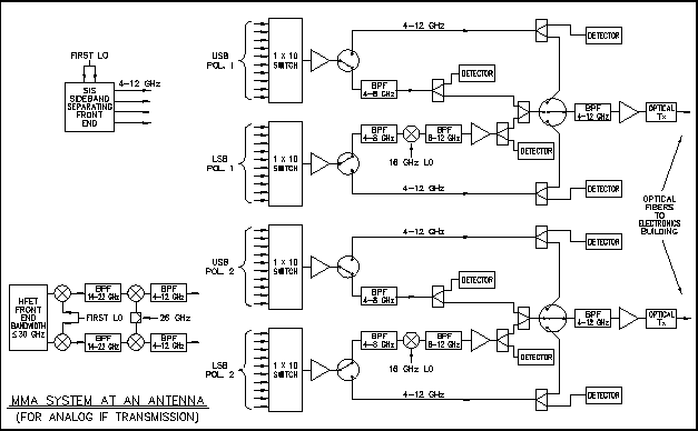
Figure 2: IF System at an Antenna
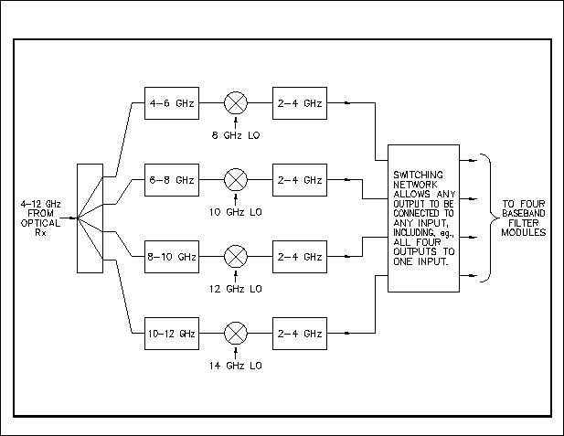
Figure 3: IF Demultiplexing Unit
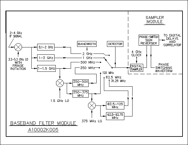
Figure 4: Baseband Converter and Digital Sampler
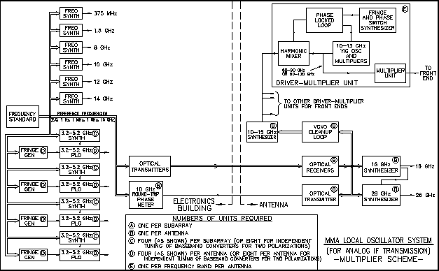
Figure 5: LO System with Multipliers for First LO
Postscript version of Figure 5 may be easier to read.
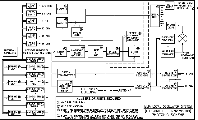
Figure 6: LO System with Photonic First LO
Postscript version of Figure 6 may be easier to read.